Everything you wanted to know about Metaoptics but were too afraid to ask
By Olov von Hofsten |
Metaoptics brings something truly new and innovative to optics. The possibility to exchange a large number of lenses into a thin, flat surface sounds almost too good to be true. Metaoptics has been around for a while now, and we now see many applications introduced by Samsung, Google, ST, and Apple (ref 1). But if they are truly so fantastic, why do we not see them everywhere? And why are our cameras still sticking out from our otherwise super-thin mobile devices? Is there something stopping metalenses from truly taking off? This and other basics on metaoptics is the topic of this article.
WHAT IS A METALENS?
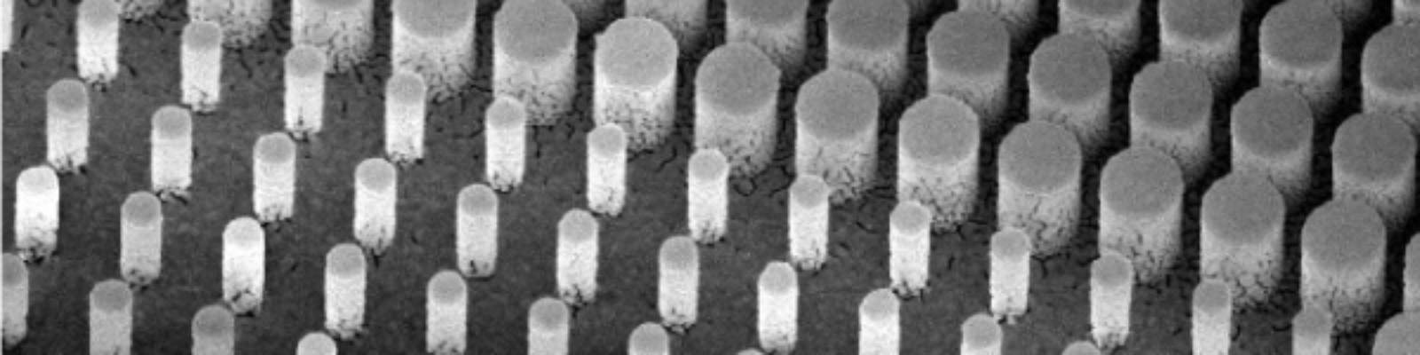
A metalens is a nanostructured element that adds a phase shift to light by using nanometer-sized objects. The structures are so small that they are smaller than the wavelength of light and therefore the light wave sees a material characterized by an average over a number of nanostructrues. This is a bit simplified; there is some advanced math magic needed to fully understand the function. But, by varying the shape, size and spacing of the nanostructures, different phases can be added to the incoming light. Most of the early work behind metalenses was done by the Capasso group at Harvard, and a lot of great information can be found there on applications and function. https://capasso.seas.harvard.edu/metasurfaces-and-flat-optics. An example of structures can be seen in figure 1.
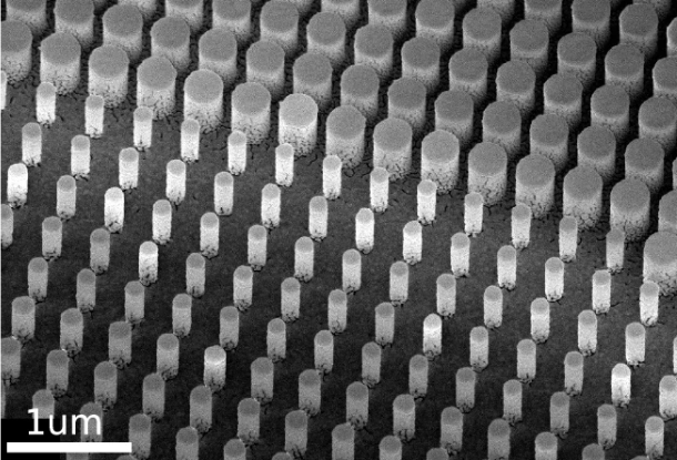
Figure 1: Cylinder nanostructures building a metalens (ref 2).
WHY USE A METALENS?
There are a number of benefits for using a metalens compared to a refractive lens. But there are also drawbacks. It is important to understand this so that you will know if metalenses are useful for your application. Let’s start with the benefits.
- The possibility to replace multiple lenses with a single element. This enables smaller form factor systems and, in some cases, also lower cost. A great example is the Metaeye camera from NILT (although it is actually two metasurfaces) (ref 3).
- The ability to add functionality like polarization control or wavelength-dependent phase. This has resulted in some interesting applications like the polarization camera from Metalenz (ref 4) which enables a much safer form of face identification, and in new use of microlenses for camera chips.
- Excellent scalability for mass production. Ready for high-volume manufacturing in semiconductor foundries and easily integrated with CMOS-compatible nanofabrication processes.
- Temperature stability. In e.g automotive and space, this is essential. In other markets, not as much.
Here are the drawbacks.
- Size limits. This is not only for cost reasons, the manufacturing of nanometer-sized structures over large areas presents problems. For a standard size lens you need billions of meta-atoms.
- Wavelength dependence. Most applications of metalenses are limited to single wavelength with less than 10 nm bandwidth. Center wavelength tolerance is slightly easier and can be larger but larger bandwidth increases cost and complexity. In theory, you can have a metalens work for much wider wavelength ranges but this has not been commercially available so far. At least for a realistic budget.
- Focusing efficiency is not 100%! Transmission losses from light going to higher orders but also due to imperfections in the nanostructure fabrication.
- Stray light. Depending on the design, the structures may cause light to go in higher order directions which causes stray light.
- Cost. Manufacturing of prototypes are expensive, about 5-10k€ for a single 2×2 mm lens. For a 4×4 mm lens, cost are 20-40 k€. This is because the protoypes are manufactured by e-beam lithography and therefore the cost is directly proportional to the time it takes to write the structures, usually silicone on glass. In volume, the cost per unit is small but tooling costs are expensive. However, this is also true for conventional lenses.
- Limits to the phase gradient. The higher the phase gradient, meaning higher NA, the more difficult it will be to manufacture the metalens. There is no hard limit but instead the scattering into higher orders will increase with the NA.
HOW DO YOU DESIGN A METALENS?
Metalenses are comprised of metasurfaces which can be modelled as a phase map in Zemax. Once this phase map/surface is optimized, it can be the input into a program like Lumerical or PlanOpSim where the surface is transferred to a nanostructred surface where the phase values are replaced by some type of nanopillars. The shape, size and spacing of the pillars can be optimized and software like PlanOpSim have libraries that make this easier. When you have the new structure you can simualate the light propagation through the structures and then use it as an input into your larger optical system.
HOW DO YOU MAKE A METALENS?
For prototypes, the structures are manufactured by electron beam lithography in Silicon on glass. For larger volumes, nanoimprinting by a premade tool is used and this requires some additional steps. See figure 2!
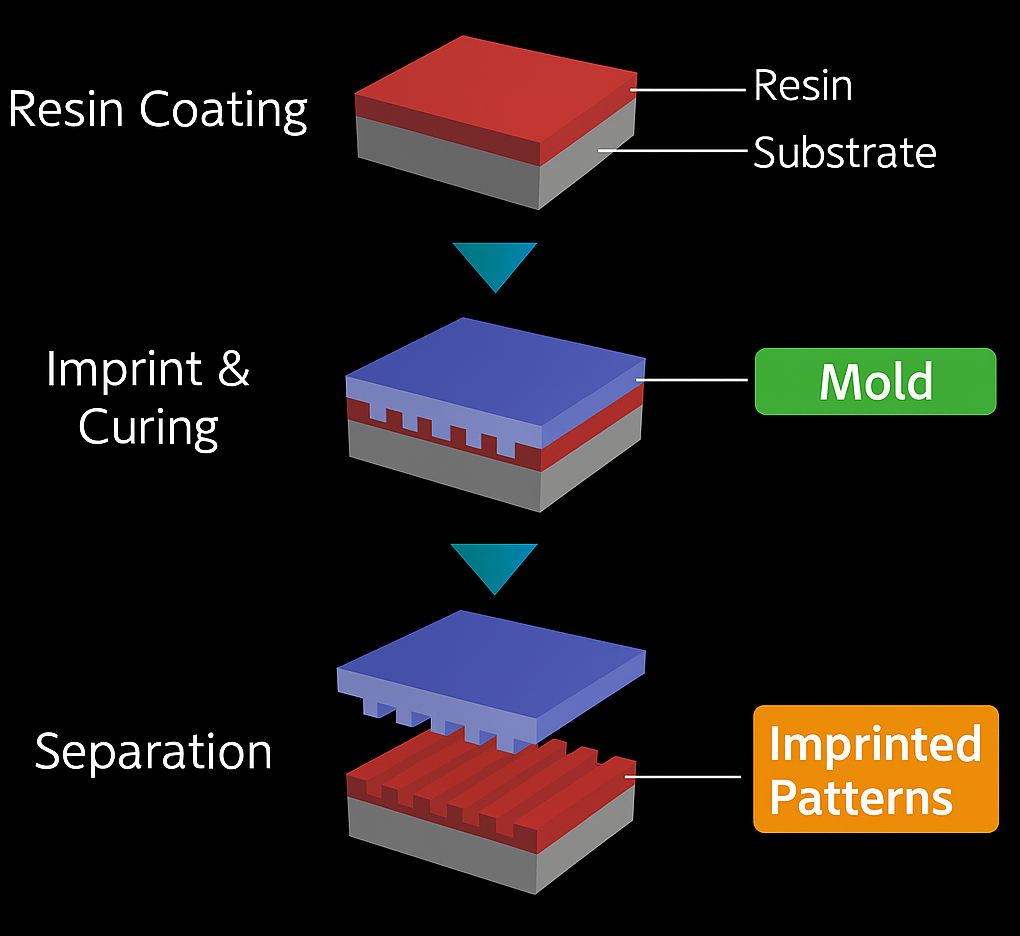
Figure 2. Imprint process for metastructures manufactured in volume (taken from ref 5)
To get more clarity in the use of metalenses, me and my colleague Peter came up with a number of basic questions, that we think a lot of people could be interested in. We asked Lieven Penninck at PlanOpSim (ref 5), an expert in the field, these questions.
- Compared to your expectation three years ago, has metalenses taken off in the way you expected?
Lieven: This is somewhat subjective but I think meta-lenses have met expectations in the sense that they are now present in large volume consumer electronics like smartphones. Simultaneously the understanding of meta-surfaces have matured and some inflated expectations like completely achromatic lenses are no longer being proposed.
- Nanostructures – that sounds very fragile and sensitive to both shock and vibration, as well as scratching, dirt and contamination. Is it?
Lieven: In isolation the nanostructures are sensitive but the industry has solved this by developing encapsulation methods. - Will metalenses replace refractive lenses eventually?
Lieven: A metalens most important strength is to create functionality that is difficult or impossible by refractive lenses. For example combining multiple lenses or making ultra-compact optics. In other aspects like broadband operation a refractive lens remains a better solution. So a general replacement of refractive lenses is unlikely. - Is there a volume limit when it becomes worth it to use a metalens instead of refractive lenses?
Lieven: There is a significant NRE cost involved with mass manufacturing meta-surfaces. Amortizing that cost requires sufficiently large volumes. The threshold where it makes economical sense to use a meta-surface is rapidly evolving and application specific. It makes sense here to look at the evolutions that have occurred in electronics and photonic integrated circuits where standardization and mask sharing has served to lower the NRE cost. - What size is reasonable for a metalens prototype? And what does a single metalens prototype lens cost?
Lieven: This depends on the wavelength range and size. A good starting point ais a few 1000 euro. - Do metalenses need to be AR coated?
Lieven: For proof of concepts the meta-lens will work without AR coating. For application AR coating is best used. This can be combined with encapsulation (see 2). - What is a reasonable number on the transmission of a metalens?
Lieven: With AR coating 98-99%. - How do metalenses compare to diffraction optics?
Lieven: Meta-lenses are a related technology to diffractive optics. And shares its ability to control wavefronts as well as the inherent diffractive dispersion behaviour. Meta-lenses differentiate from DOEs by easily creating multi-level phase control (contrary to binary type DOEs), ability to incorporate function like polarization control. - When will we see a metalens in our smartphone cameras?
Lieven: Today. Yole development has done teardowns of Samsung S23 and Ipad pro and found they use meta-lenses for some cameras. It’s important these are laser illuminated applications, so the diffractive nature of the meta-lens is not an issue.
REFERENCES
- https://www.yolegroup.com/technology-outlook/metasurfaces-break-through-turning-speculation-into-reality/
2. Egede Johansen, V., Gür, U.M., Martínez-Llinás, J. et al. Nanoscale precision brings experimental metalens efficiencies on par with theoretical promises. Commun Phys 7, 123 (2024). https://doi.org/10.1038/s42005-024-01598-6
3. NILT: https://www.nilt.com/products/meta-optics/metaeye-camera/
4. Metalenz: https://metalenz.com/polareyes-polarization-imaging-system/polar-id/)
5. PlanOpSim: https://planopsim.com/