
Using the EMVA1288 standard
By Linus Frantzich |
Comparing the performance of two image sensors can almost be an administrative, rather than a technical task. Most image sensor metrics depend on exposure time, gain, lens performance and temperature to name a few. Including all conditions and comparing using the same conditions exponentially increases the administrative effort. At times, even the definition of these metrics is not clear, especially when given by image sensor suppliers.
In this 3-part blog post we will travel down this rabbit hole and hopefully end up in a wonderful world of comparable digital image sensors on the other side.
In the first part of this blog, we will briefly introduce the CMOS image sensor. Secondly, we outline image sensor performance metrics and finally, in the third part, we will go more into the details of the EMVA1288 standard.
Part 1 – CMOS image sensor introduction
The CMOS image sensor (CIS) is a photon-counting device. It’s divided into an array of picture elements (pixels) where each pixel counts the photons it detects over its area, which is usually on the micrometer-scale. It does this over a time period, usually called the exposure time. Since the pixel is only counting photons, not measuring their energy, a color filter over each pixel is needed to sort photons by color. The most common color filter array (CFA) is the Bayer RGGB pattern. It consists of red, blue and two green pixels per 2×2 pixels. Although many variants of the CIS exist, the most common type is the voltage mode type, which is used in many consumer products and more recently in the automotive industry. This blog post will focus on this type of image sensor.
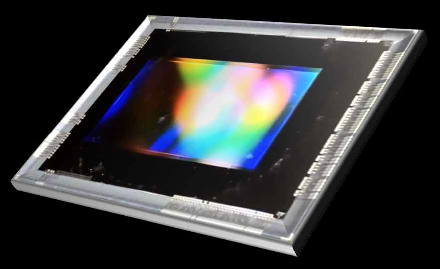
Figure 1: A photo of a CMOS image sensor
Since the photon is a difficult particle to measure directly, a set of solid-state devices in each pixel are used to transform photons into electrons and measure them. The collected electrons’ charge can be measured using a capacitor. The voltage over the capacitor is related to the charge by the capacitance. In a modern CIS, the four-transistor (4T) pixel architecture is common. It employs four transistors per pixel. The pinned photodiode is used to convert photons into electrons. A transistor is used to transfer the charge in the photodiode to a storage node. The other transistors are used to reset the pixel, essentially making it ready for a new exposure, and to select and read-out the collected electrons after the exposure, see figure 2.
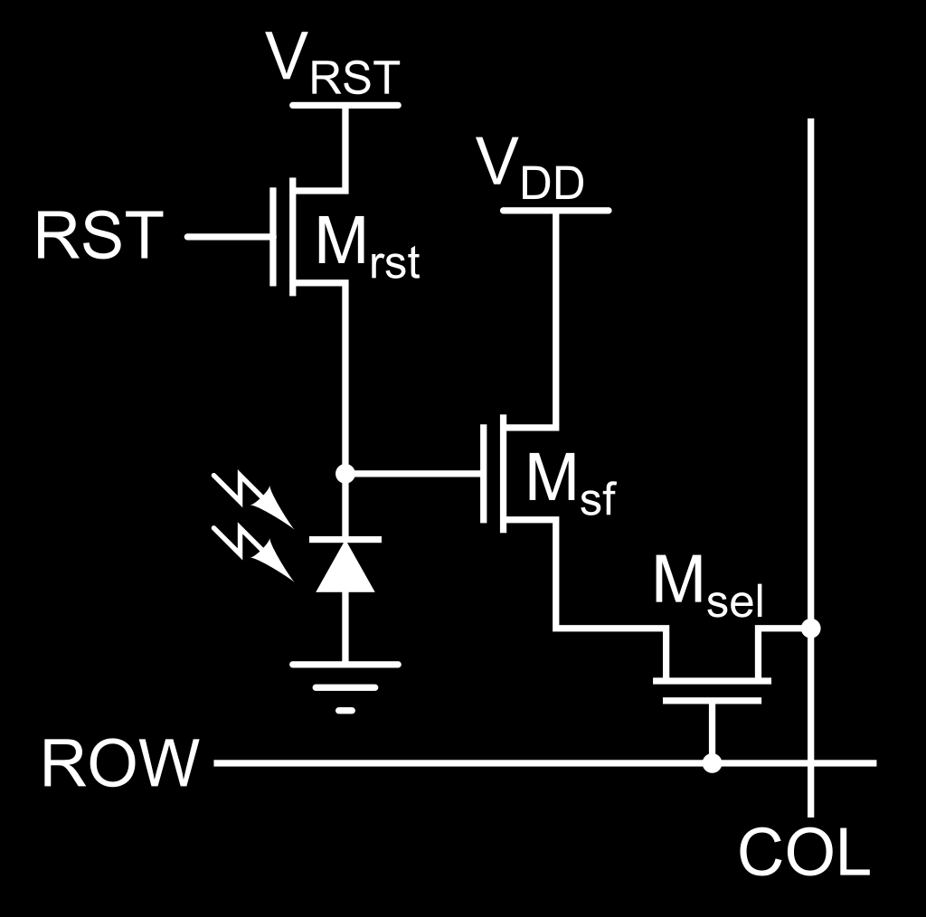
Figure 2: Simplified schematic of the 4T architecture. The pinned photodiode is indicated by a diode symbol. The reset transistor has the symbol “RST”. The read-out transistor, also called source follower, is denoted Msf. The select transistor can be seen connecting to the row and column bus. Source: Wikipedia “Active pixel sensor” https://en.wikipedia.org/wiki/Active-pixel_sensor.
The voltage over the capacitor in each pixel can be amplified and is then converted to a digital value using an analog-to-digital converter (ADC). The precision of the ADC determines the bit-depth of the digital value. Using internal circuits on the image sensor, the digital signal is output, and each pixel digital value can be assigned to a specific pixel in an image. In figure 3, the signal chain from photons to digital number is illustrated.
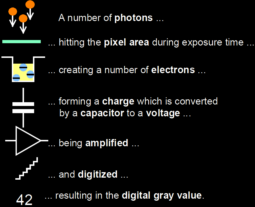
Figure 3: Photon to digital number, step-by-step conversion. Source: EMVA1288 4.0 Linear “https://www.emva.org/wp-content/uploads/EMVA1288Linear_4.0Release.pdf”
Photons from the imaged scene generate electrons, called photoelectrons, which are the quantity of the scene that we are looking to measure. Quantum mechanics limits us to measure it precisely due to photon shot noise. Simply put, photon shot noise is the uncertainty in the number of photons arriving on the pixel during an exposure, which we can’t affect. It’s usually the dominating noise source in well-lit conditions as the noise increases with the square root of the signal. Luckily, that also means that the higher the signal level, the higher the signal to noise ratio (SNR) will be. In contrast, in low-light conditions noise generated by the image sensor will dominate the noise.
Adding to photon shot noise, the process of sampling photoelectrons introduces additional noise from several contributors in the image sensors, for example thermal noise, 1/f noise, quantization noise, etc. There are several techniques implemented in sensors to reduce these noise sources. Instead of going more into details of each noise source, standards like EMVA1288 focus on measuring and classifying the noise by its characteristics.
Part 2 – Image sensor performance metrics
One of the most important image sensor metrics is noise. Noise is quantified by the standard deviation from the mean or expected number of electrons. The general term for the signal generated in the absence of light is dark signal and its statistical variation is called dark noise.
Noise may affect pixels, rows and columns differently. For example, if pixel reset is done for the entire row, all pixels in that row can have similar offsets from the reset action. Therefore, it’s common to divide pixel into these contributions; pixel, row, column and the total. Dark noise can be divided into two categories: temporal and spatial.
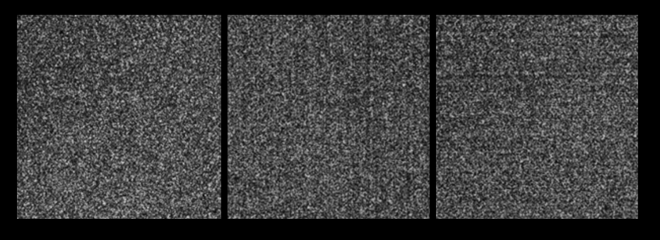
Figure 4: Random noise (left), random noise with visible column noise (middle), random noise with visible row noise (right)
Temporal dark noise is the random variation from measuring the dark signal in each pixel. It’s manifested in variations of a pixel value from frame to frame. Like photon shot noise, it too has its origin in quantum mechanics. Spatial dark noise (sometimes referred to as fixed pattern noise) is a static signal pattern and can be quantified with the same quantity as temporal noise except it doesn’t change with time. Since the underlying process is not random, noise is not the correct term, instead EMVA1288 adopted the term non-uniformity. Other than its magnitude, non-uniformities can also be measured by their spatial distributions, which may be gradual from one side of the image sensor to the other, be periodic or outliers, which for example, is the case for defect or broken pixels.
Other than noise metrics, image sensors can be benchmarked on the number of electrons a pixel can hold without saturating, known as full well capacity. The ability to effectively convert photons to electrons, called the quantum efficiency (QE) is also commonly measured as a function of photon wavelength. This is especially relevant for color sensors with RGB, IR or other types of bandpass filters. The quantities mentioned so far can be used to compute other important metrics, for example, dynamic range.
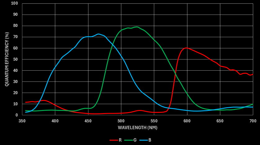
Figure 5: Example of quantum efficiency curves for sensor with Bayer RGGB CFA.
For some applications, image sensors are measured with a lens. To avoid effects of lens vignetting and other field-dependent effects, only the optical center should be considered in these cases. Measuring with a lens makes metrics more relevant for the end use case, but at the same time, it makes them dependent on the lens specification. Comparing image sensors measured with different lenses can increase the complexity further. SNR is a metric that is impacted by the lens since the amount of signal is directly dependent on the brightness, or f-number, of the lens.
Part 3 – Image sensor metrics in EMVA1288
The metrics in the previous part have been commonplace in image sensor benchmarking for a long time. ISO standards such as ISO15739:2023 address some of them, others are described in other standards. If only there was a standard that more directly to the point encapsulated all the metrics in one easy-to-implement standard!
So far in this blog post, EMVA1288 has been mentioned but not introduced. The European Machine-Vision Association is a non-profit, non-commercial association representing the machine vision industry in Europe. The EMVA1288 standard aims to define a unified method to measure, compute and present sensor metrics. It is free to use, and a Python reference implementation is available on GitHub. The standard doesn’t include long explanations (like this blog post does) about image sensors, the purpose or background of measurements, instead the image sensor is treated as a black box. Electrons come in, noise is added, electron charge is converted to voltage and to the closest integer number by an ADC. In a few chapters all important image sensor metrics are covered. The final chapters focus on clarifications and methods for practical implementation, as well as description of how to report the results. Besides the results, the operating point of the sensor needs to be included. This includes conditions like temperature, gain, exposure time and more.
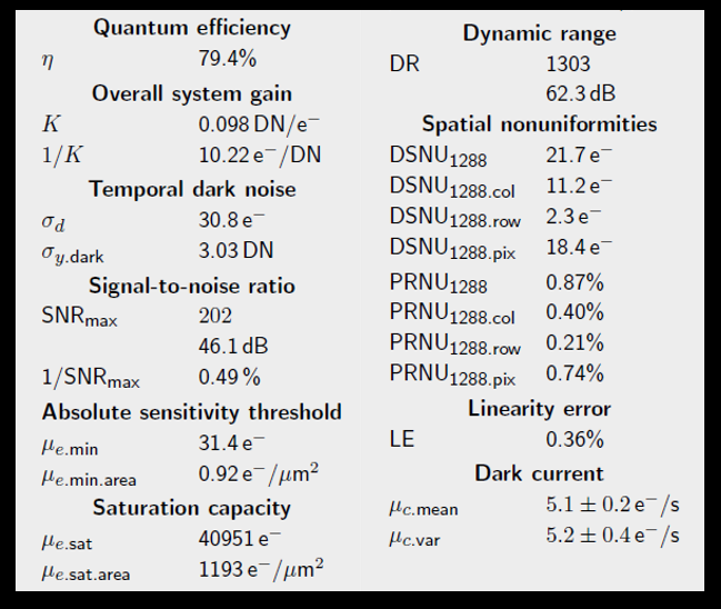
Figure 6: Example of EMVA1288 results template. Source: EMVA1288 4.0 Linear “https://www.emva.org/wp-content/uploads/EMVA1288Linear_4.0Release.pdf”
Metrics covered by the EMVA but not yet mentioned in this blog post, include absolute sensitivity threshold, dark current, photo response non-uniformity (PRNU) and linearity error (LE).
Parts not included in the EMVA standard yet are dark current non-uniformity (DCNU) and full well capacity. Hopefully in coming editions, these metrics will be included. Recently, EMVA announced that they will lift the standard to an ISO level standard.
Conclusion
The lack of clear metrics and (possibly) lack of competence on the receiving end has given image sensor suppliers the freedom to arbitrarily define their metrics to score higher than their competitors. For example, it’s not uncommon for the dynamic range of a sensor to be specified by the ratio of the highest and lowest digital number of the ADC. While dynamic range could be defined this way, it’s only a measurement of the ADC bit depth. By specifying EMVA1288 dynamic range, it’s the range starting from the digital number needed to achieve SNR=1 to the digital number where a maximum of 0.1-0.2% pixels is saturated due to photon shot noise. It both makes comparison easy and represents a number true to the original intent: “the range of usable output values”. At the same time, it will have dependencies on, for example, analog gain which makes the comparison more complicated than comparing ADC bit depth. Both dynamic range using only temporal and total noise (spatial + temporal) can be reported.
The solution is to request suppliers to measure their sensors using EMVA1288 in pre-defined conditions for temperature, gain and exposure time. Even then, suppliers can choose to measure their best sensors that are not representative of a batch of random sensors. They can also use power management and environments that are not practically possible to implement in product. The alternative is to measure sensors in an in-house or independent (unbiased) lab. This adds complexity since access to sensors and demo boards is needed. Setting up a camera lab has been described in a previous blog post. Eclipse Optics offers evaluation of image sensors using EMVA1288 metrics and as well as analysis of how these metrics impact a product or use case application. Don’t hesitate to contact us for more information.

